
|
Jupyter at Bryn Mawr College |
|
|
| Public notebooks: /services/public/dblank / CS240 Computer Organization / 2017-Fall / Notebooks | |||
3.5 The Concept of Memory
[These sections are based on your textbook, Introduction to Computing Systems: From Bits & Gates to C & Beyond (second edition), by Yale N. Patt & Sanjay J. Patel, McGraw Hill Publishers, 2004.]
We now describe one of the most important structures in the electronic digital computer, its memory. We explore how memory fits into the basic scheme of computer processing, and you will see throughout the rest of the book and indeed the rest of your work with computers how important the concept of memory is to computing.
Memory is made up of a (usually large) number of locations, each uniquely identifiable and each having the ability to store a value. We refer to the unique identifier associated with each memory location as its address. We refer to the number of bits of information stored in each location as its addressability. For example, an advertisement for a personal computer might say, "This computer comes with 16 megabytes of memory." Actually, most ads generally use the abbreviation 16 MB. This statement means, as we will explain momentarily, that the computer system includes 16 million memory locations, each containing 1 byte of information.

3.5.1 Address Space
We refer to the total number of uniquely identifiable locations as the memory's address space. A 16 MB memory, for example, refers to a memory that consists of 16 million uniquely identifiable memory locations.
Actually, the number 16 million is only an approximation, due to the way we identify memory locations. Since everything else in the computer is represented by sequences of Os and 1 s, it should not be surprising that memory locations are identified by binary addresses as well. With n bits of address, we can uniquely identify 2n locations. Ten bits provide 1,024 locations, which is approximately 1,000. If we have 20 bits to represent each address, we have 220 uniquely identifiable locations, which is approximately 1 million. Thus 16 mega really corresponds to the number of uniquely identifiable locations that can be specified with 24 address bits. We say the address space is 224, which is exactly 16,777,216 locations, rather than 16,000,000, although we colloquially refer to it as 16 million.
3.5.2 Addressability
The number of bits stored in each memory location is the memory's addressability. A 16 megabyte memory is a memory consisting of 16,777,216 memory locations, each containing 1 byte (i.e., 8 bits) of storage. Most memories are byte-addressable. The reason is historical; most computers got their start processing data, and one character stroke on the keyboard corresponds to one 8-bit ASCII character, as we learned in Chapter 2. If the memory is byte-addressable, then each ASCII code occupies one location in memory. Uniquely identifying each byte of memory allowed individual bytes of stored information to be changed easily.
Many computers that have been designed specifically to perform large scientific calculations are 64-bit addressable. This is due to the fact that numbers used in scientific calculations are often represented as 64-bit floating point quantities. Recall that we discussed the floating point data type in Chapter 2. Since scientific calculations are likely to use numbers that require 64 bits to represent them, it is reasonable to design a memory for such a computer that stores one such number in each uniquely identifiable memory location.
5.1 The ISA: Overview
The ISA specifies all the information about the computer that the software has to be aware of. In other words, the ISA specifies everything in the computer that is available to a programmer when he/she writes programs in the computer's own machine language. Thus, the ISA also specifies everything in the computer that is available to someone who wishes to translate programs written in a high-level language like C or Pascal or Fortran or COBOL into the machine language of the computer.
The ISA specifies the memory organization, register set, and instruction set, including opcodes, data types, and addressing modes.
NOTE: Languages like Python and Java have their own, higher-level virtual machine instruction set. This allows the lower-level language (often written in C) to be easily ported from one instruction set to another.
5.1.1 Memory Organization
The LC-3 memory has an address space of 216 (i.e., 65,536) locations, and an addressability of 16 bits. Not all 65,536 addresses are actually used for memory locations, but we will leave that discussion for Chapter 8. Since the normal unit of data that is processed in the LC-3 is 16 bits, we refer to 16 bits as one word, and we say the LC-3 is word-addressable.
Cycles
[Based on information in Chapter 4.]
As we will see, THE CONTROL UNIT consists of all the structures needed to manage the processing that is carried out by the computer. Its most important structure is the Finite State Machine (FSM), which directs all the activity. Processing is carried out step by step, or rather, clock cycle by clock cycle.
The Clock
[Based on information in Chapter 3.]
Frequently, the mechanism that triggers the transition from one state to the next is a clock circuit. A clock circuit, or, more commonly, a clock, is a signal whose value alternates between 0 volts and some specified fixed voltage. In digital logic terms, a clock is a signal whose value alternates between 0 and 1.
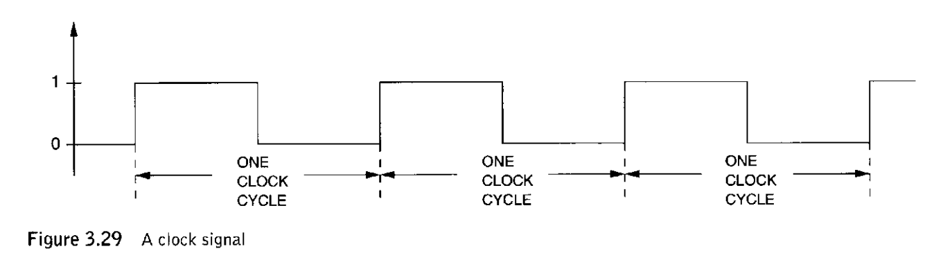
The clock is used to synchronized all of the electronics in the computer circuitry. As we shall see, a FSM has a series of states that it progresses through to perform different functions. Two such functions are:
- retrieving information from a register (1 cycle)
- retrieving information from a memory location (many cycles, depending on instruction)
5.1.2 Registers
Since it usually takes far more than one machine cycle to obtain data from memory, the LC-3 provides (like almost all computers) additional temporary storage locations that can be accessed in a single machine cycle.
The most common type of temporary storage locations and the one used in the LC-3 is the general purpose register set. Each register in the set is called a general purpose register (GPR). Registers have the same property as memory locations in that they are used to store information that can be retrieved later. The number of bits stored in each register is usually one word. In the LC-3, this means 16 bits.
Registers must be uniquely identifiable. The LC-3 specifies eight GPRs, each identified by a 3-bit register number. They are referred to as RO, R1, R2, R3, R4, R5, R6, and R7.
Instruction Variations
So far, we have seen the following instructions:
- ADD - 0001 DST SRC 1 VVVVV
- HALT - 1111 0000 00100101
- AND - 0101 DST SRC 1 VVVVV
- NOT - 1001 DST SRC 111111
We will refer to each of the bits of an instruction by the numbering from right to left, like this:
15 14 13 12 11 10 9 8 7 6 5 4 3 2 1 0surrounded by brackets. So, [0] is the right-most bit, and [15] is the left-most bit.
A range of bits will be referred to using [LEFT:RIGHT]. So, [3:0] is the 4 right-most bits, and [15:12] is the left-most bits (e.g., the instruction).
ADD and AND operate on the contents of registers and an immediate value VVVVV. Recall that the value VVVVV is sign-extended before any operation. So that:
01111will be sign-extended to be these 16 bits:
0000000000001111Likewise:
10000will be sign-extended to be these 16 bits:
1111111111110000However, AND and ADD can also operate on the contents of a register by using the 0 (non-immediate) flag:
- ADD - 0001 DST SRC 0 00 SRC
- AND - 0101 DST SRC 0 00 SRC
The second SRC operand for both ADD and AND instructions can be specified by either register mode (0) or as an immediate operand (1). Bit [5] determines which is used. If bit [5] is 0, then the second source operand uses a register, and bits [2:0] specify which register. In that case, bits [4:3] are set to 0 to complete the specification of the instruction.
In these versions of the instructions, we change the 1 flag to a 0, and change VVVVV to 00SRC. This SRC will use the contents of the SRC register. So the instruction:
0001 001 010 0 00 011will use the contents of register 011 (R3) and ADD that to the contents of register 010 (R2) and store the results in register 001 (R1).
Let's try out these instructions:
ADD the contents of R0 + R0 and store to R1:
.ORIG x3000

0001 001 000 0 00 000 ;; ADD R1 <= R0 + R0
1111 0000 00100101 ;;

.END
%exe
That is a little hard to test without have numbers besides zero. Let's store the following into the registers:
- R1 gets 1
- R2 gets 2
- R3 gets 3
- R4 gets 4
- R5 gets 5
- R6 gets 6
And then ADD all of the registers together and store the result into R0.
.ORIG x3000
0001 0010 0010 0001 ;; ADD R1 <- R0 + 1
0001 010 000 1 00010 ;; ADD R2 <- R0 + 2
0001 011 000 1 00011 ;; ADD R3 <- R0 + 3
0001 100 000 1 00100 ;; ADD R4 <- R0 + 4
0001 101 000 1 00101 ;; ADD R5 <- R0 + 5
0001 110 000 1 00110 ;; ADD R6 <- R0 + 6

1111 0000 00100101 ;; HALT
.END
%dump
%exe
.ORIG x3000
0001 001 000 1 00001 ;; ADD R1 <- R0 + 1
0001 010 000 1 00010 ;; ADD R2 <- R0 + 2
0001 011 000 1 00011 ;; ADD R3 <- R0 + 3
0001 100 000 1 00100 ;; ADD R4 <- R0 + 4
0001 101 000 1 00101 ;; ADD R5 <- R0 + 5
0001 110 000 1 00110 ;; ADD R6 <- R0 + 6

0001 000 000 0 00 001 ;; ADD R0 <- R0 + R1
0001 000 000 0 00 010 ;; ADD R0 <- R0 + R2
0001 000 000 0 00 011 ;; ADD R0 <- R0 + R3
0001 000 000 0 00 100 ;; ADD R0 <- R0 + R4
0001 000 000 0 00 101 ;; ADD R0 <- R0 + R5
0001 000 000 0 00 110 ;; ADD R0 <- R0 + R6

1111 0000 00100101 ;; HALT
.END
%exe
Program Counter and Debugging the LC-3
The program counter, or PC for short, is a register that keeps track of the line of code that we are executing. It starts out with the value given by .ORIG, and increments by one right before each instruction.
We can't see the PC increment, unless we using the single-step debugging tools.
Let's see these in action. Let's use the first program that we wrote above to initialize the registers to values 1 through 6. First we assemble the program:
.ORIG x3000
0001 001 000 1 00001 ;; ADD R1 <- R0 + 1
0001 010 000 1 00010 ;; ADD R2 <- R0 + 2
0001 011 000 1 00011 ;; ADD R3 <- R0 + 3
0001 100 000 1 00100 ;; ADD R4 <- R0 + 4
0001 101 000 1 00101 ;; ADD R5 <- R0 + 5
0001 110 000 1 00110 ;; ADD R6 <- R0 + 6

1111 0000 00100101 ;; HALT
.END
Now, instead of %exe executing the code, we will set the PC register manually, and %step through the code:
%pc x3000
%step
The first part of the output shows that the PC is getting x3001, and then we execute ADD R1, R0, #1. This is a shorthand for our instruction, where #1 stands for immediate mode, value of 1.
The result is that R1 gets the value x0001. In addition, the N, Z, and P registers get 0, 0, and 1 respectively. The NZP registers are assigned a value based on the last operation:
- NZP <= (0, 0, 1) ;; if the last operation was a positive number
- NZP <= (0, 1, 0) ;; if the last operation was zero
- NZP <= (1, 0, 0) ;; if the last operation was a negative number
============================================================
Stepping...  => read, <= write, (Instructions/Cycles):
============================================================
    PC <= x3001
(1/6) ADD R1, R0, #1 [1] (x3001*: x1221)
    R1 <= x0001
    NZP <= (0, 0, 1)
The last part of the output shows all of the registers:
============================================================
Registers:
============================================================
PC: x3001
N: 0 Z: 0 P: 1
R0: x0000 R1: x0001 R2: x0000 R3: x0000
R4: x0000 R5: x0000 R6: x0000 R7: x0000%step
Every time we use %step, we increment the PC, and execute the next instruction. You have access to the following metacommands:
LC3 Interactive Magic Directives:
 %help                              - shows this help message
 %bp [clear | SUSPENDHEX]           - show, clear, or set breakpoints
 %cont                              - continue running
 %dump [STARTHEX [STOPHEX]]         - list memory in hex
 %exe                               - execute the program
 %mem HEXLOCATION HEXVALUE          - set memory
 %pc HEXVALUE                       - set PC
 %reg REG HEXVALUE                  - set register REG to HEXVALUE
 %regs                              - show registers
 %reset                             - reset LC3 to start state
 %step                              - increment PC, execute the next instruction
Memory Instructions
The LC-3 contains seven instructions that move information to and from memory:
- LD
- LDR
- LDI
- LEA
- ST
- STR
- STI
The format of the load and store instructions is as follows:
| [15:12] | [11:9] | [8:0] |
|---|---|---|
| OPCODE | DST or SRC | ADDRESS GENERATION BITS |
Data movement instructions require two operands, a source and a destination. The source is the data to be moved; the destination is the location where it is moved to. One of these locations is a register, the second is a memory location or an input/output device. In this chapter the second operand will be assumed to be in memory.
Bits [11:9] specify one of these operands, the register. If the instruction is a load, DST refers to the destination register that will contain the value after it is read from memory (at the completion of the instruction cycle). If the instruction is a store, SRC refers to the register that contains the value that will be written to memory.
Bits [8:0] contain the address generation bits. That is, bits [8:0] encode information that is used to compute the 16-bit address of the second operand. In the case of the LC-3's data movement instructions, there are four ways to interpret bits [8:0]. They are collectively called addressing modes. The opcode specifies how to interpret bits [8:0]. That is, the LC-3's opcode specifies which addressing mode should be used to obtain the operand from bits [8:0] of the instruction.
5.3.1 PC-Relative Mode
| Instruction | [15:12] | [11:9] | [8:0] |
|---|---|---|---|
| LD | 0010 | DST | VVVVVVVVV |
| ST | 0011 | SRC | VVVVVVVVV |
LD (opcode = 0010) and ST (opcode = 0011) specify the PC-relative addressing mode. This addressing mode is so named because bits [8:0] of the instruction specify an offset relative to the PC. The memory address is computed by sign-extending bits [8:0] to 16 bits, and adding the result to the incremented PC.
The incremented PC is the contents of the program counter after it has been incremented. If a load, the memory location corresponding to the computed memory address is read, and the result loaded into the register specified by bits [11:9] of the instruction.
LD DST <= PC+VVVVVVVVV
ST SRC => PC+VVVVVVVVV.ORIG x3000
0010 000 000000000 ;; LD R0 <= PC+000000000
1111 1111 1111 1111 ;; xFFFF
.END
%pc x3000
%step
.ORIG x3000
0010 000 111111111 ;; LD R0 <= PC+-1
.END
%pc x3000
%step
5.3.2 Indirect Mode
| Instruction | [15:12] | [11:9] | [8:0] |
|---|---|---|---|
| LDI | 1010 | DST | VVVVVVVVV |
| STI | 1011 | SRC | VVVVVVVVV |
LDI (opcode — 1010) and STI (opcode = 1011) specify the indirect addressing mode. An address is first formed exactly the same way as with LD and ST. However, instead of this address being the address of the operand to be loaded or stored, it contains the address of the operand to be loaded or stored. Hence the name indirect. Note that the address of the operand can be anywhere in the computer's memory, not just within the range provided by bits [8:0] of the instruction as is the case for LD and ST. The destination register for the LDI and the source register for STI, like all the other loads and stores, are specified in bits [11:9] of the instruction.
LDI DST <= M[PC+VVVVVVVVV]
STI SRC => M[PC+VVVVVVVVV].ORIG x3000
1010 000 000000000
0011 0000 0000 0000
.END
%pc x3000
%step
.ORIG x3000
1011 000 000000000 ;; STI R0 => M[PC+0]
0011 0000 0000 0000
.END
%pc x3000
%step
%dump x3000
5.3.3 Base+offset Mode
| Instruction | [15:12] | [11:9] | [8:6] | [5:0] |
|---|---|---|---|---|
| LDR | 0110 | DST | BSE | OFFSET |
| STR | 0111 | SRC | BSE | OFFSET |
LDR (opcode = 0110) and STR (opcode = 0111) specify the Base+offset addressing mode. The Base+offset mode is so named because the address of the operand is obtained by adding a sign-extended 6-bit offset to a base register. The 6-bit offset is literally taken from the instruction, bits [5:0]. The base register is specified by bits [8:6] of the instruction.
The Base+offset addressing uses the 6-bit value as a 2's complement integer between —32 and +31. Thus it must first be sign-extended to 16 bits before it is added to the base register.
LDR DST <= M[BASE + OFFSET]
STR SRC => M[BASE + OFFSET].ORIG x3000
0110 000 000 000001
.END
%pc x3000
%step
5.3.4 Immediate Mode
| Instruction | [15:12] | [11:9] | [8:0] |
|---|---|---|---|
| LEA | 1110 | DST | VVVVVVVVV |
The fourth and last addressing mode used by the data movement instructions is the immediate (or, literal) addressing mode. It is used only with the load effective address (LEA) instruction. LEA (opcode = 1110) loads the register specified by bits [11:9] of the instruction with the value formed by adding the incremented program counter to the sign-extended bits [8:0] of the instruction. The immediate addressing mode is so named because the operand to be loaded into the destination register is obtained immediately, that is, without requiring any access of memory.
The LEA instruction is useful to initialize a register with an address that is very close to the address of the instruction doing the initializing.
LEA DST <= PC + VVVVVVVVV.ORIG x3000
1110 000 000000000
.END
%pc x3000
%step
5.3.5 An Example
We conclude our study of addressing modes with a comprehensive example. Assume the contents of memory locations x30F6 through x30FC are as shown in Figure 5.10 (and below), and the PC contains x30F6. We will examine the effects of carrying out the instruction cycle seven consecutive times.
.ORIG x30F6
1110 001 111111101 ;; LEA R1, #-3
0001 010001101110
0011 010111111011
0101 010010100000
0001 010010100101
0111 010001001110
1010 011111110111
.END
%pc x30F6
The PC points initially to location x30F6. That is, the content of the PC is the address x30F6. Therefore, the first instruction to be executed is the one stored in location x30F6. The opcode of that instruction is 1110, which identifies the load effective address instruction (LEA). LEA loads the register specified by bits [11:9] with the address formed by sign-extending bits [8:0] of the instruction and adding the result to the incremented PC. The 16-bit value obtained by sign-extending bits [8:0] of the instruction is xFFFD. The incremented PC is x30F7. Therefore, at the end of execution of the LEA instruction, R1 contains x30F4, and the PC contains x30F7.
%step
The second instruction to be executed is the one stored in location x30F7. The opcode 0001 identifies the ADD instruction, which stores the result of adding the contents of the register specified in bits [8:6] to the sign-extended immediate in bits [4:0] (since bit [5] is 1) in the register specified by bits [11:9]. Since the previous instruction loaded x30F4 into R1, and the sign-extended immediate value is xOOOE, the value to be loaded into R2 is x3102. At the end of execution of this instruction, R2 contains x3102, and the PC contains x30F8. R1 still contains x30F4.
%step
The third instruction to be executed is stored in x30F8. The opcode 0011 specifies the ST instruction, which stores the contents of the register specified by bits [11:9] of the instruction into the memory location whose address is computed using the PC-relative addressing mode. That is, the address is computed by adding the incremented PC to the 16-bit value obtained by sign-extending bits [8:0] of the instruction. The 16-bit value obtained by sign-extending bits [8:0] of the instruction is xFFFB. The incremented PC is x30F9. Therefore, at the end of execution of the ST instruction, memory location x30F4 contains x3102, and the PC contains x30F9.
%step
At x30F9, we find the opcode 0101, which represents the AND instruction. After execution, R2 contains the value 0, and the PC contains x30FA.
%step
At x30FA, we find the opcode 0001, signifying the ADD instruction. After execution, R2 contains the value 5, and the PC contains x30FB.
%step
At x30FB, we find the opcode 0111, signifying the STR instruction. The STR instruction (like the LDR instruction) uses the Base+offset addressing mode. The memory address is obtained by adding the contents of the register specified by bits [8:61 (the BASE register) to the sign-extended offset contained in bits [5:0]. In this case, bits [8:6] specify R1. The contents of R1 are still x30F4. The 16-bit sign-extended offset is xOOOE. Since x30F4 + xOOOE is x3102, the memory address is x3102. The STR instruction stores into x3102 the contents of the register specified by bits [11:9], that is, R2. Recall that the previous instruction (at x30FA) stored the value 5 into R2. Therefore, at the end of execution of this instruction, location x3102 contains the value 5, and the PC contains x30FC.
%step
At x30FC, we find the opcode 1010, signifying the LDI instruction. The LDI instruction (like the STI instruction) uses the indirect addressing mode. The memory address is obtained by first forming an address as is done in the PC-relative addressing mode. In this case, the 16-bit value obtained by sign-extending bits [8:0] of the instruction is xFFF7. The incremented PC is x30FD. Their sum is x30F4, which is the address of the operand address. Memory location x30F4 contains x3102. Therefore, x3102 is the operand address. The LDI instruction loads the value found at this address (in this case 5) into the register identified by bits [11:9] of the instruction (in this case R3). At the end of execution of this instruction, R3 contains the value 5 and the PC contains x30FD.
%step